


 3Likes
Transponder Design
 08-29-2013 | 01:10 AM
#151
Tech Apprentice
Joined: Jan 2013
Posts: 61
From: Schoonebeek
@edeca: I work on my own code now and found almost all ASM instructions only use 1 cycle for the 12F683. What do I overlook? If each of my ASM instructions that I need to generate the ID indeed only use a single cycle, do I understand correct for 5MHz clock I may use 4 instructions? The instructions outise the period were the ID is generated towards the GPIO may use more instructions as this is just for generating the random interval in between the sending of the ID's. Can you respond to me?
@edeca: Already solved, each ASM instruction is executed by an Internal instruction cycle clock which is FOSC/4.
This indeed puts some pressure in being creative to set the GPIO in as less as possible ASM instructions...
No need to reply anymore!
@edeca: Already solved, each ASM instruction is executed by an Internal instruction cycle clock which is FOSC/4.
This indeed puts some pressure in being creative to set the GPIO in as less as possible ASM instructions...
No need to reply anymore!
Last edited by PA3EXV; 08-29-2013 at 04:37 AM. Reason: Already found the answer by digging through the datasheet...
 08-29-2013 | 09:13 AM
#152
Tech Initiate
Joined: Jun 2013
Posts: 20
@edeca: I work on my own code now and found almost all ASM instructions only use 1 cycle for the 12F683. What do I overlook? If each of my ASM instructions that I need to generate the ID indeed only use a single cycle, do I understand correct for 5MHz clock I may use 4 instructions? The instructions outise the period were the ID is generated towards the GPIO may use more instructions as this is just for generating the random interval in between the sending of the ID's. Can you respond to me?
@edeca: Already solved, each ASM instruction is executed by an Internal instruction cycle clock which is FOSC/4.
This indeed puts some pressure in being creative to set the GPIO in as less as possible ASM instructions...
No need to reply anymore!
@edeca: Already solved, each ASM instruction is executed by an Internal instruction cycle clock which is FOSC/4.
This indeed puts some pressure in being creative to set the GPIO in as less as possible ASM instructions...
No need to reply anymore!
Using a 5Mhz crystal without the PLL you can quite happily use a run of pure ASM to generate the modulated carrier. You get a whole one instruction cycle (four crystal cycles) per modulation period. This means you can really only toggle the bits using xor or set the whole port. These instructions only take one clock cycle. You can't use any branching.
This does mean that you are limited by program memory if you want more than one identifier. You also can't easily include other data in the transponder code, such as battery status or temperature.
With the 4x PLL you get four instructions per modulated bit (sixteen crystal cycles). This allows use of branching and you can therefore do some slightly more clever ASM. I think I got my code down to 5 instructions to send the whole 90 bit transponder code. The code is calculated beforehand and stored in a buffer.
This makes it much easier to calculate the message and include other data, then send it using a generic loop.
10-04-2013 | 12:45 PM
#153
Tech Apprentice
Joined: Jan 2013
Posts: 61
From: Schoonebeek
Hi all,
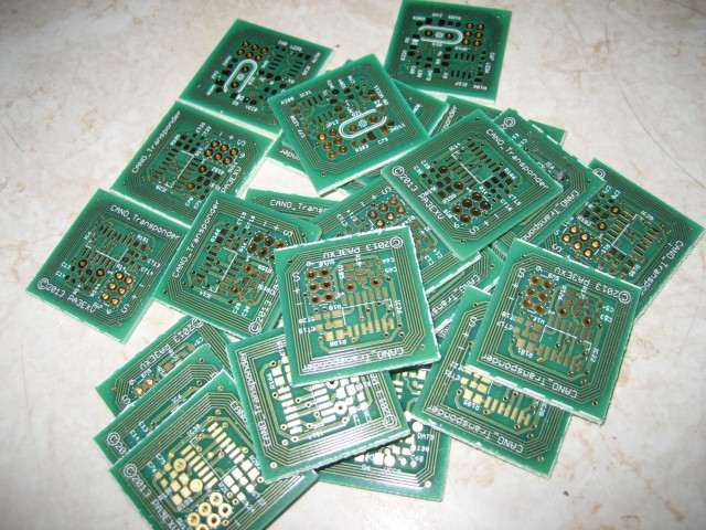
This week my 4-layered PCB for the transponder came in. I already shared the design with you, and now it's time to show the hardware.
Here you see the PCB's still without the SMD components, ready for placement of resistors, capacitors, the 74AC86, a 5MHz crystal and the 12F683:
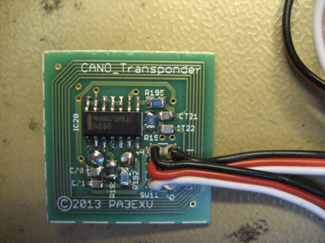
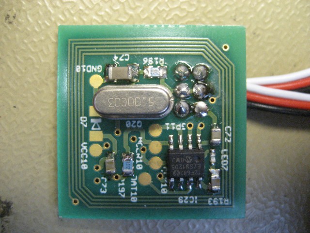
After mounting the components, the 2-sided PCBA looks like this:
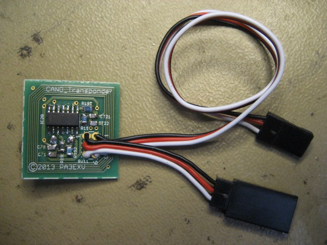
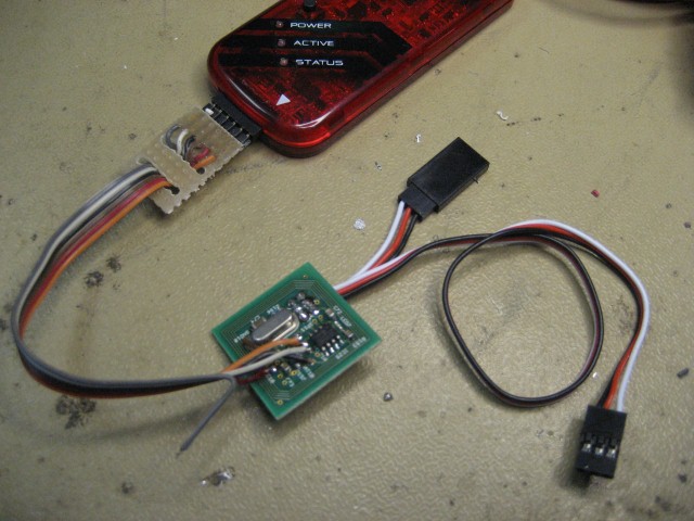
I have chosen to insert the transponder into one of the servo-wires in my car (gas/break). That is why a longer cable (male_plug) and a shorter wire (female_plug) is soldered into the transponder PCBA:
To program the transponder in circuit, I have 5 gold-plated pads at the back-side of the PCB, Later I will build a small jig onto which the transponder_PCBA can be placed for programming. It will use small spring-loaded testpins so I don't need to solder wires to every PCBA:
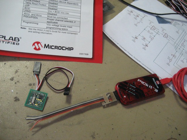
For now I soldered the PICKit3 programmer for the 12F683 directly to the first transponder to see if all worked as expected...And it did!
I now must continue on the software inside the transponder to have a blinking LED. I must use interrupt service routines which is a new programming technique for me to explore. By using this, the data-transmissions are not disrupted by the blinking LED. Let's see what comes out. For now the transponder sends its DATA as in the proto board I made earlier and can be seen in my posts in the decoder portion.
This week my 4-layered PCB for the transponder came in. I already shared the design with you, and now it's time to show the hardware.
Here you see the PCB's still without the SMD components, ready for placement of resistors, capacitors, the 74AC86, a 5MHz crystal and the 12F683:
After mounting the components, the 2-sided PCBA looks like this:
I have chosen to insert the transponder into one of the servo-wires in my car (gas/break). That is why a longer cable (male_plug) and a shorter wire (female_plug) is soldered into the transponder PCBA:
To program the transponder in circuit, I have 5 gold-plated pads at the back-side of the PCB, Later I will build a small jig onto which the transponder_PCBA can be placed for programming. It will use small spring-loaded testpins so I don't need to solder wires to every PCBA:
For now I soldered the PICKit3 programmer for the 12F683 directly to the first transponder to see if all worked as expected...And it did!
I now must continue on the software inside the transponder to have a blinking LED. I must use interrupt service routines which is a new programming technique for me to explore. By using this, the data-transmissions are not disrupted by the blinking LED. Let's see what comes out. For now the transponder sends its DATA as in the proto board I made earlier and can be seen in my posts in the decoder portion.
10-04-2013 | 01:01 PM
#154
Tech Initiate
Joined: Jun 2013
Posts: 20
Another option is to simply count transmissions and change the LED state when a variable rolls over. Something like the following pseudo-code:
1) Send data
2) Random delay
3) Increment variable i
4) If i == 0, LED equals the opposite of the LED (use XOR)
5) Repeat
I did this for my development version and it worked very well.
10-04-2013 | 05:07 PM
#156
 10-05-2013 | 08:15 AM
#157
Tech Initiate
Joined: Jun 2013
Posts: 20
10-07-2013 | 12:27 PM
#158
Tech Apprentice
Joined: Jan 2013
Posts: 61
From: Schoonebeek
After I finished my first transponder I still feld it could be improved for the range a bit...It turned out the used tuning-capacitors not quite matched the coil in my PCB.
With help of my collegue at work (JWZ) using a Network-Analyser, we measured my inductance at 13.5uH @ 5MHz. This was the startingpoint to simulate the circuit. The driver has an output_resistance of 33 Ohm on both sides (2 x 33 = 66 Ohm), the series-resistors have both 82 Ohm resulting in 217 Ohm source impedance. To match the 13.5uH we found the capacitors (see Smith-chart...). The simulated capacitor then were not exactly available as usual and after some finetuning the coil showed nice resonance at 5MHz. The lower picture show the Spectrum-Analyser were I have the transponder measured by sweep the frequency in 100kHz steps by using an external RF-Generator instead of the 5MHz cryatal on the PCB. One pin of the 74AC86 drivers is tied to GND, the other to VCC to enable the RF into the coil.
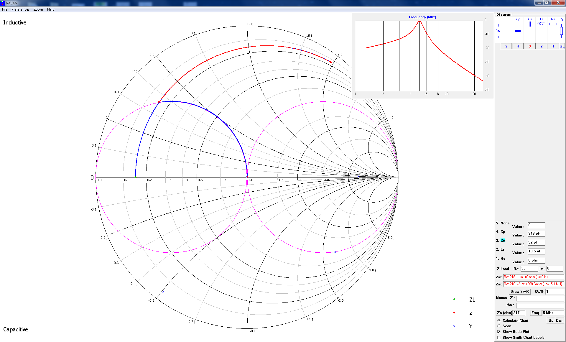
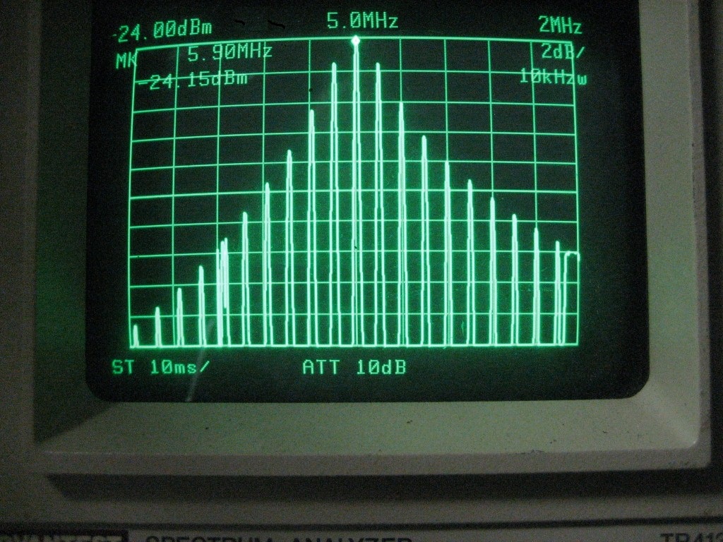
With help of my collegue at work (JWZ) using a Network-Analyser, we measured my inductance at 13.5uH @ 5MHz. This was the startingpoint to simulate the circuit. The driver has an output_resistance of 33 Ohm on both sides (2 x 33 = 66 Ohm), the series-resistors have both 82 Ohm resulting in 217 Ohm source impedance. To match the 13.5uH we found the capacitors (see Smith-chart...). The simulated capacitor then were not exactly available as usual and after some finetuning the coil showed nice resonance at 5MHz. The lower picture show the Spectrum-Analyser were I have the transponder measured by sweep the frequency in 100kHz steps by using an external RF-Generator instead of the 5MHz cryatal on the PCB. One pin of the 74AC86 drivers is tied to GND, the other to VCC to enable the RF into the coil.
10-14-2013 | 01:11 PM
#159
Tech Apprentice
Joined: Jan 2013
Posts: 61
From: Schoonebeek
@EDECA: That did the job, using a counter inside the loop and check for a certain bit is set, then toggle the LED at GP0. By selecting what bit to check I am able to change the blink_rate....NICE! I must admit however, it took a few evenings to understand the machine_code commands available in the 12F683 like the 'BTFSC'-command which I now used to determine the LED to toggle or not. Now that the LED blinks AND the transponder still transmit in burst-mode and above that the decoder still recognizes the preamble and ID, I am so happy today, I wanted to let you know :-)
@Howard: I removed from one of the 4-layered PCB's the trace that makes the 20 windings and replaced it on top of the PCB-surface by thin wire with again 20 windings. This gaves better results in the distance towards the receiver_loop after re-adjusting the 2 tuning_C's. I think the Q of the PCB_coil in my case is not matching the purpose. Any way, the PCB's I have still is very usefull to hold the crystal, the PIC and the driver. The small amount of boards i need for our club is easy enough to fabricate by using a wire_coil in the transponder. A too high Q gives lots of issues in phase_inverion. There is so much energy inside the coil, it is not easy to swap phase within 1 period. I tried adding a resistor across the PCB_coil to damp out the high Q, but I feel this is not the correct way to go; First generate a lot of energy and because of the high Q waste it in a resistor (4 - 10KOhm)...If I have time I look into this further. I guess your face showes a smile because you have been here already few months ago and found the same issues...
Now we start to implement a decoder PIC that will communicate over USB towards my scoring software next to the CPLD that already is functional for the decoding part. If that goes well, we have a system that can be tested in real life with one of our cars. Let's hop winter stays away for a couple of weeks.
10-14-2013 | 02:55 PM
#160
I removed from one of the 4-layered PCB's the trace that makes the 20 windings and replaced it on top of the PCB-surface by thin wire with again 20 windings. This gaves better results in the distance towards the receiver_loop after re-adjusting the 2 tuning_C's. I think the Q of the PCB_coil in my case is not matching the purpose. Any way, the PCB's I have still is very usefull to hold the crystal, the PIC and the driver. The small amount of boards i need for our club is easy enough to fabricate by using a wire_coil in the transponder.
A too high Q gives lots of issues in phase_inverion. There is so much energy inside the coil, it is not easy to swap phase within 1 period. I tried adding a resistor across the PCB_coil to damp out the high Q, but I feel this is not the correct way to go; First generate a lot of energy and because of the high Q waste it in a resistor (4 - 10KOhm)...If I have time I look into this further. I guess your face showes a smile because you have been here already few months ago and found the same issues...
There's absolutely nothing wrong with changing the tank Q with either series or parallel resistance. It's actually the best way to do it, rather than to rely on other losses that may not be as controlled or repeatable.
12-09-2013 | 10:56 AM
#161
Tech Initiate
Joined: Apr 2013
Posts: 46
That's almost correct!
The method is called Binary Phase Shift Keying (BPSK). There are many descriptions of it on the internet, but here's a quick description particular to the example you gave:
A logic 1 is indicated by ANY reversal in the carrier phase. (This is just a convention I am using. We could just as easily say that the carrier reversal indicates a logic 0.) The initial carrier phase, before data is sent, is unimportant.
First, the data stream must be preceded for a short time with the carrier turned on to give the tank circuit time to "ring up" to full amplitude, and time for the phase detector in the decoder to generate a first valid output. Then a start bit (an initial logic "1") is sent to indicate the beginning of the data stream.
So the sequence is:
1. pin 5 = low, pin 6 = low, tank circuit is not not driven and does not radiate.
2. pin 5 = high, pin 6 = low, initial ring up for tank circuit
3. pin 5 = low, pin 6 = high for one machine cycle (4 carrier periods) sends the start bit
4. No changes for 3 more machine cycles (12 carrier periods) sends "000"
5. pin 5 = high, pin 6 = low for one machine cycle (4 carrier periods) sends a logic "1"
6. No changes for 3 more machine cycles (12 carrier periods) sends "000"
Between 5 and 6, you don't need change value off pin 5 and pin 6 ?
thanks.
12-09-2013 | 01:41 PM
#164
Tech Initiate
Joined: Apr 2013
Posts: 46
How many "status messages" has a AMB transponder ?
A AMB transponder has a "ID message" which is repeated 3 times.
Is it possible to record a status messages group, and send it this group with another transponder "ID message"?
thanks.
A AMB transponder has a "ID message" which is repeated 3 times.
Is it possible to record a status messages group, and send it this group with another transponder "ID message"?
thanks.
12-09-2013 | 04:34 PM
#165
There are seven different status messages on each of the AMB transponders I have examined. All seven appear to be different from transponder to transponder, so I never tried using an ID message from one transponder with the status messages from a different transponder. But that would be an interesting experiment!