


 8Likes
Lap Timing Decoder
 04-01-2013 | 04:19 AM
#166

The software for separating transponder ID messages from status messages, and sending only the ID messages to the PC, is operational. Despite being quite complex, the software functioned on the first try.
The first photo shows 10 transponders gathered around a small testing loop. This is a worst-case scenario, and in fact I wasn�t counting on the software being able to determine which messages are for ID and save them to the list in RAM in this situation... While it does take a few seconds for all the IDs to be determined and saved, it eventually happens. This is a pleasant surprise.
The first photo shows 10 transponders gathered around a small testing loop. This is a worst-case scenario, and in fact I wasn�t counting on the software being able to determine which messages are for ID and save them to the list in RAM in this situation... While it does take a few seconds for all the IDs to be determined and saved, it eventually happens. This is a pleasant surprise.
My initial belief that having 10 transponders in the loop at the same time would prevent determination of ID messages was, in fact, correct. I found a glitch in the software that made it possible, but only rarely would also recognize a status message as an ID message (which would have alerted me to the problem). Now that this glitch has been corrected, IDs can be determined for only about 5 transponders in the loop at the same time.
Again, this has no effect on normal operation, where each transponder ID is recognized as each car individually passes through the loop (we call this �checking in�). When all of the IDs have been recognized, then all 10 transponders can be in the loop simultaneously with no ill effects.
 04-04-2013 | 01:47 PM
#167
The Digital Phase Detector (DPD) is now operational.
This thread started with an account of the first iteration of the DPD, and my main concern then was eliminating spurious pulses in the detector output created when the transponder carrier edges would occur in a different sample period than expected due to mismatched clock frequencies between the DPD and the transponder. My original approach was to use three individual phase detectors that would sample at different times, then combine the outputs with a majority logic gate so that a spurious pulse from any single detector would be suppressed. I wasn’t entirely successful!
The new approach is to use a single detector, but suppress spurious pulses by requiring that there be pulses in at least two out of three successive sample times to result in a final output from the DPD.
Here’s the schematic, followed by a short description:
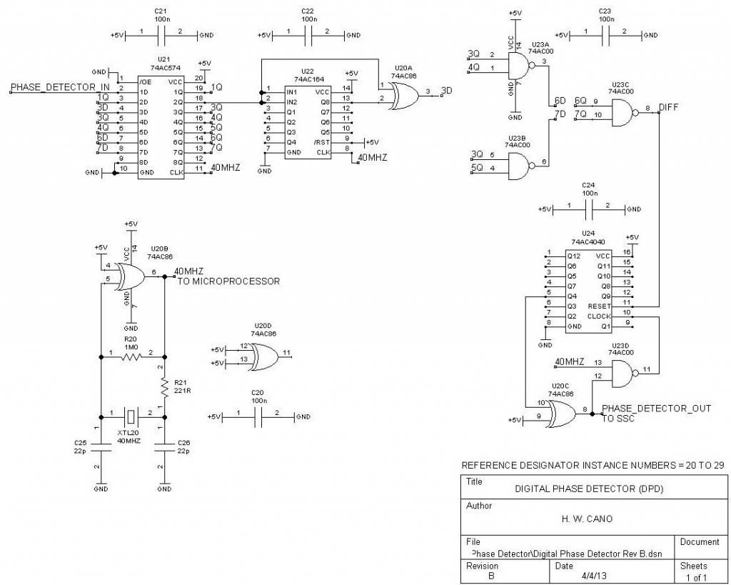
U20B and associated components create a 40 MHz clock signal for the DPD. (This can also be divided down to 20 MHz for use as the microprocessor clock, shown on a different schematic sheet.)
The output from the Phase Detector Input Amplifier feeds two series-connected D flip-flops in U21 (1D/1Q/2D/2Q) that sample the transponder’s 5 MHz carrier eight times per carrier cycle. The series connection reduces timing inaccuracy due to metastability.
The sampled, synchronized signal feeds one input of XOR gate U20A (the “heart” of the detector) and shift register U22. U22 delays the signal by eight sample clock periods (one full transponder carrier cycle). U20A then compares the original signal with the delayed signal, and its output goes high if they do not match. The XOR gate output is then re-synchronized to the sample clock by U21 flip flop 3D/3Q.
Two more sections of U21, 4D/4Q and 5D/5Q, delay the 3Q output by an additional one and two sample clock periods, respectively.
NAND gates U23A and U23B will generate valid (low) outputs if the XOR output was high for either two successive sample clock periods, or high for a first and third sample clock period, respectively. The outputs are again re-synchronized to the sample clock by U21 flip flops 6D/6Q and 7D/7Q. U23C then ORs the gate outputs together to create the “DIFF” signal. “DIFF” goes high only when the transponder carrier has swapped phases (phase modulation). Single, spurious pulses from U20A never appear at “DIFF”.
Counter U24 and associated gates form a pulse stretcher to transform one or several closely-spaced DIFF pulses into a single, longer pulse at “PHASE_DETECTOR_OUT”. Any positive pulse at “DIFF” resets U24’s Q4 output. U20C inverts this to give “PHASE_DETECTOR_OUT”. U23D gates the 40 MHz clock to enable counting by U24 whenever “PHASE_DETECTOR_OUT” is high. After eight sample clock periods, Q4 goes high, “PHASE_DETECTOR_OUT” goes low, and counting ceases. If more than one pulse appears at “DIFF” before Q4 goes high, the counter will reset and the pulse length at “PHASE_DETECTOR_OUT” will be extended.
EDIT: For the latest schematics, see post 206:
http://www.rctech.net/forum/12118142-post206.html
This thread started with an account of the first iteration of the DPD, and my main concern then was eliminating spurious pulses in the detector output created when the transponder carrier edges would occur in a different sample period than expected due to mismatched clock frequencies between the DPD and the transponder. My original approach was to use three individual phase detectors that would sample at different times, then combine the outputs with a majority logic gate so that a spurious pulse from any single detector would be suppressed. I wasn’t entirely successful!
The new approach is to use a single detector, but suppress spurious pulses by requiring that there be pulses in at least two out of three successive sample times to result in a final output from the DPD.
Here’s the schematic, followed by a short description:
U20B and associated components create a 40 MHz clock signal for the DPD. (This can also be divided down to 20 MHz for use as the microprocessor clock, shown on a different schematic sheet.)
The output from the Phase Detector Input Amplifier feeds two series-connected D flip-flops in U21 (1D/1Q/2D/2Q) that sample the transponder’s 5 MHz carrier eight times per carrier cycle. The series connection reduces timing inaccuracy due to metastability.
The sampled, synchronized signal feeds one input of XOR gate U20A (the “heart” of the detector) and shift register U22. U22 delays the signal by eight sample clock periods (one full transponder carrier cycle). U20A then compares the original signal with the delayed signal, and its output goes high if they do not match. The XOR gate output is then re-synchronized to the sample clock by U21 flip flop 3D/3Q.
Two more sections of U21, 4D/4Q and 5D/5Q, delay the 3Q output by an additional one and two sample clock periods, respectively.
NAND gates U23A and U23B will generate valid (low) outputs if the XOR output was high for either two successive sample clock periods, or high for a first and third sample clock period, respectively. The outputs are again re-synchronized to the sample clock by U21 flip flops 6D/6Q and 7D/7Q. U23C then ORs the gate outputs together to create the “DIFF” signal. “DIFF” goes high only when the transponder carrier has swapped phases (phase modulation). Single, spurious pulses from U20A never appear at “DIFF”.
Counter U24 and associated gates form a pulse stretcher to transform one or several closely-spaced DIFF pulses into a single, longer pulse at “PHASE_DETECTOR_OUT”. Any positive pulse at “DIFF” resets U24’s Q4 output. U20C inverts this to give “PHASE_DETECTOR_OUT”. U23D gates the 40 MHz clock to enable counting by U24 whenever “PHASE_DETECTOR_OUT” is high. After eight sample clock periods, Q4 goes high, “PHASE_DETECTOR_OUT” goes low, and counting ceases. If more than one pulse appears at “DIFF” before Q4 goes high, the counter will reset and the pulse length at “PHASE_DETECTOR_OUT” will be extended.
EDIT: For the latest schematics, see post 206:
http://www.rctech.net/forum/12118142-post206.html
Last edited by howardcano; 06-11-2013 at 08:15 AM.
04-07-2013 | 05:48 AM
#168
Tech Initiate
Joined: Dec 2012
Posts: 48
The Digital Phase Detector (DPD) is now operational.
This thread started with an account of the first iteration of the DPD, and my main concern then was eliminating spurious pulses in the detector output created when the transponder carrier edges would occur in a different sample period than expected due to mismatched clock frequencies between the DPD and the transponder. My original approach was to use three individual phase detectors that would sample at different times, then combine the outputs with a majority logic gate so that a spurious pulse from any single detector would be suppressed. I wasn�t entirely successful!
The new approach is to use a single detector, but suppress spurious pulses by requiring that there be pulses in at least two out of three successive sample times to result in a final output from the DPD.
Here�s the schematic, followed by a short description:
U20B and associated components create a 40 MHz clock signal for the DPD. (This can also be divided down to 20 MHz for use as the microprocessor clock, shown on a different schematic sheet.)
The output from the Phase Detector Input Amplifier feeds two series-connected D flip-flops in U21 (1D/1Q/2D/2Q) that sample the transponder�s 5 MHz carrier eight times per carrier cycle. The series connection reduces timing inaccuracy due to metastability.
The sampled, synchronized signal feeds one input of XOR gate U20A (the �heart� of the detector) and shift register U22. U22 delays the signal by eight sample clock periods (one full transponder carrier cycle). U20A then compares the original signal with the delayed signal, and its output goes high if they do not match. The XOR gate output is then re-synchronized to the sample clock by U21 flip flop 3D/3Q.
Two more sections of U21, 4D/4Q and 5D/5Q, delay the 3Q output by an additional one and two sample clock periods, respectively.
NAND gates U23A and U23B will generate valid (low) outputs if the XOR output was high for either two successive sample clock periods, or high for a first and third sample clock period, respectively. The outputs are again re-synchronized to the sample clock by U21 flip flops 6D/6Q and 7D/7Q. U23C then ORs the gate outputs together to create the �DIFF� signal. �DIFF� goes high only when the transponder carrier has swapped phases (phase modulation). Single, spurious pulses from U20A never appear at �DIFF�.
Counter U24 and associated gates form a pulse stretcher to transform one or several closely-spaced DIFF pulses into a single, longer pulse at �PHASE_DETECTOR_OUT�. Any positive pulse at �DIFF� resets U24�s Q4 output. U20C inverts this to give �PHASE_DETECTOR_OUT�. U23D gates the 40 MHz clock to enable counting by U24 whenever �PHASE_DETECTOR_OUT� is high. After eight sample clock periods, Q4 goes high, �PHASE_DETECTOR_OUT� goes low, and counting ceases. If more than one pulse appears at �DIFF� before Q4 goes high, the counter will reset and the pulse length at �PHASE_DETECTOR_OUT� will be extended.

 04-08-2013 | 05:19 AM
#169
Our readers might be interested in seeing what's happening on the other side of the world:
http://vk.com/club17646479
04-09-2013 | 03:07 AM
#171

 :
: 04-09-2013 | 03:29 AM
#175
Tech Initiate
Joined: Dec 2012
Posts: 48
And I think its time to share software for emulation of amb20:
https://www.dropbox.com/s/pkyigvfnohbzqel/amb20.rar
password - "payalneg"
This is very simple programm writen on Codevision v2.0. For programmers no trouble to recreate schematics. Mcu works on external crystal 7.3728Mhz. Also thera 32.768kHz crystal on TOSC.
https://www.dropbox.com/s/pkyigvfnohbzqel/amb20.rar
password - "payalneg"
This is very simple programm writen on Codevision v2.0. For programmers no trouble to recreate schematics. Mcu works on external crystal 7.3728Mhz. Also thera 32.768kHz crystal on TOSC.
 04-09-2013 | 08:28 AM
#177
I’m about the right age for that, too. When 74HC logic was brand new… I wasn’t.
Others have already pointed out that most of this design could go into an FPGA, but 74HC logic still has the advantages of being both very cheap and still made by multiple manufacturers. (There’s nothing worse than designing with a single-sourced part, then having that part be discontinued by the manufacturer.) And, of course, it doesn’t need to be programmed!
I should give a word of warning: there are a few high-speed portions in this design (particularly the Digital Phase Detector) that may not function properly on a solderless breadboard. The layout should be kept as small as possible, and could use a ground plane, even for prototyping.
04-09-2013 | 12:18 PM
#178
Tech Initiate
Joined: Dec 2012
Posts: 48
I should give a word of warning: there are a few high-speed portions in this design (particularly the Digital Phase Detector) that may not function properly on a solderless breadboard. The layout should be kept as small as possible, and could use a ground plane, even for prototyping.
04-10-2013 | 12:29 AM
#179
Tech Rookie
Joined: Mar 2013
Posts: 8
04-10-2013 | 11:38 AM
#180
Tech Initiate
Joined: Feb 2013
Posts: 29
Hi, I just finished receiver with mcu (STM32). I am directly sampling square wave from limiter. After decoding sending via USB to PC (for now) So far works ok, sampling is done at 20MHz. Have to check how to calculate crc to make sure message is correct. I made rf - ttl converter with ad8309 and work very good. Still have to play a bit with antenna matching. Even with not properly match dynamic range is abt 40db.
regards
Brano
regards
Brano