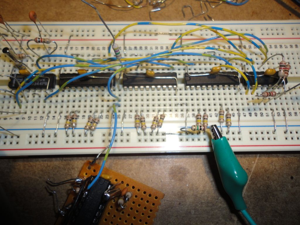
In my first post I mentioned that ambiguity of the carrier level around its zero-crossings can cause the phase detector to generate spurious pulses, and that using parallel detectors with their outputs logically ANDed together eliminates the problem. However, when a valid carrier phase inversion occurs, the ambiguity can also cause one detector to generate an output pulse that is offset enough in time to not align with the pulse from the other detector, resulting in a missed bit when their outputs are combined with the AND gate. To correct this, I have incorporated a third parallel detector, with the three detector clocks offset about 60 degrees from each other, and employed a majority logic gate that gives an output pulse whenever two or more of the detectors generate coincident pulses. It's a few more parts, but still fits on the solderless breadboard, as you can see:
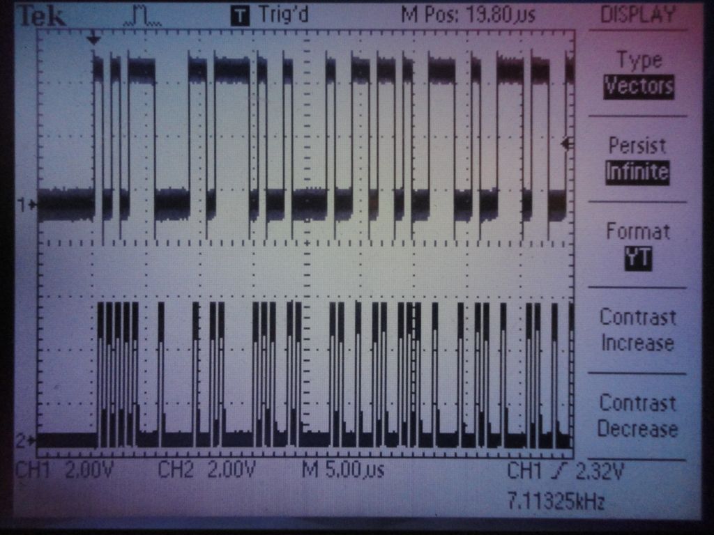
This scope shot shows the carrier modulation waveform on the top trace, and the combined detector output on the bottom trace. (The modulated carrier is applied to the detector inputs.) The scope persistence is set to "infinite" (one of the nice features of a digital scope!), and this reveals an umeasurable bit error rate (the scope triggers incorrectly every once in a while, but the output remains consistent up until that occurs).